Finally, I had finished assembling the kit. There is remaining much noise in spite of receiving the signal. So I had been worried that there were some issues.
The squelch is unstable and the squelch will close when the strong signal is coming. There is still sounding when the volume setting being 00. As the channel step is 10kHz, to listen xxx.475MHz we shall set xxx.480 or xxx.470 MHz.
To get soft sound, I added a high cut filter(1.6kΩ+0.1uF) on the audio line of LM386 input. It affected well to reduce noise. Changing ceramic filter to crystal filter is also reducing noise.
High cut filter
To stabilize squelch, I added 10uF on the SCAN signal line, but it does not affect so much.
Depending on nano VNA I adjusted the front end filter. Adding 1.5pF with at 15pF resulted in better sensitive
To adjust the front end filter
nano VNA display
Green trace: CH0 impedance of smith chart
Orange trace: CH0 reflection
Blue trace: Passband characteristics
This receiver is useful for waiting for strong signals with a deep squelch.
Thanks, IMSAI GUY for your introduction on how to assemble and adjust by YOUTUBE.
After assembled, I had adjusted and could receive the signal. However, it is very much noisy. I'm afraid of remaining some issues.
BTW I checked the passband characteristics for the front filter and LNA by using nano VNA. As LNA is 20dB gain, I inserted 20dB ATT in the front of CH1.
nano VNA connection
Comparing with the former general gain estimation, there is a -6dB gain. The result is -11.72dB.
nano VNA display
On the way to adjusting the front-end filter, the brass nuts are almost going out. We shall need the optional capacitors on paralleled 15pF.
This kit is more sensitive than the analog LO kit but SN ratio is much worse.
As there is no AGC, the signal strength feeling is not well. Also, SN ratio is low even for the strong signal.
Noise squelch circuits may be affected by static electricity. So the squelch circuit goes unstable. If you dare to use squelch, a deep setting is recommended. And you may utilize squelch only for fare strong signal only.
To get better performance for this kit, I should resolve the below issues.
1. To add the audio filter to avoid noize. 2. To stabilize the squelch circuit. 3. Audio volume issues that 2_00 is still signal being. 4. To add capacitors on the front-end circuit. 5. Is there well replacement for the squelch circuit. 6. To change 10kHz step to 25kHz step.
I'm much thanking kon for giving me the practical information of R80 kit.
I completed assembling the kit. Some noisy sound comes out from the speaker.
I resumed the voltage list of each IC node. The voltage is measured by a digital tester at DC mode. This is for simple checking to avoid mistaken wiring or parts swapping.
I also put a comment that it is noise sensitive node and the multi values for squelch ON/OFF or receiving/no signal.
I just received the kit from China and would like to start assembling it. However, there was no document with it. So I shall prepare the list by myself. Prior to soldering, I put the parts in order to check the contents being enough. I adhered the parts to the parts list to identify each other. Hurrying around is important for these complicated jobs.
parts list 1
parts list 2
Putting the parts in order
I had inserted and soldered the part in turn along with the parts list order. Accordingly, the resisters were first, nextly the ceramic capacitors, the aluminum capacitors, and the others.
After soldering I found several residual parts of the capacitors.
When I used to connect DC supply for the first time, I should use the ampere meter to detect short circuits or some mistaken.
According to the SPEC, it consumes about 110mA. At this time I found the badly reversed installation of ATT-IC and no solder parts.
It is useful for the broadcasting channel to adjust the circuit. ITM ATIS of 128.6MHz is such a signal for me.
At this step, we shall adjust the sound volume, the squelch level, and the LO basic frequency compensation.
I referred to the manual in the below section.
------------------------------------------- Press the configuration button, after release, the configuration LED light will glow red, indicating that the encoder is in volume adjustment mode. The default display is 2_ 10 after power-on. The last two digits represent the volume level. The machine can be set to 0-25. The larger the number, the volume Bigger.
Press the button again, after release, display 3_ _XX, the last two digits represent the size of the squelch threshold, this machine can be set to 0-25, the larger the number, the higher the threshold (that is, the higher level of the received signal can exit the squelch state).
Press the knob again to display 4 _33, which is the 25MHz clock frequency offset setting. The default setting is 33 and the unit is 100Hz. The default frequency is 25 000 000Hz+33*100Hz. If you find an error in the receiving frequency, you can use a frequency meter to measure the 25MHz clock frequency on the PLL board and adjust the clock frequency deviation according to the test value.
FUNCTION MODE photo 25.000MHz FREQ 128.8MHz FREQ
As the frequency meter displayed 25.00192MHz, 4_19 should be an adjustment value. However, LO was 128.82MHz for receiving 128.1MHz. So I should adjust 4_52 for getting 128.8MHz LO. I don't know why such a difference.
Squelch adjustment
As shallow squelch is hard to hear the signal, you shall set some deeper than 10.
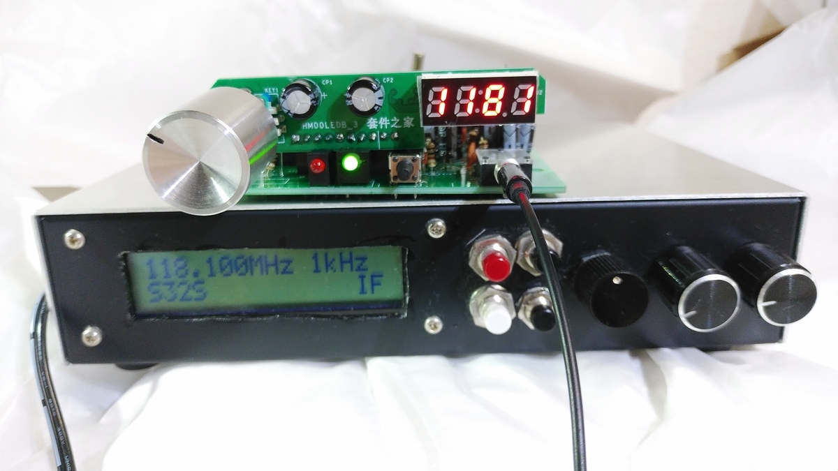
Stacked R80 on the 1st machine
I had compared R80 with 1st machine of remodeled Chinese kit(Degital LO).
After setting the parameters and adjustment for coils, nevertheless, the receiver could not demodulate a clear signal. The receiving LED was OK, and hiss noise had gone out. But I could not get a clear signal yet.
I shall need more investigation for the causes of undemanded demodulated sound.
After FM62429 variable attenuator the audio signal is going to LM386 amp. The same signal is going to the MC3661 filter amp and detector.
MC3361 is naturally the FM receiver IC and this receiver is using filter amp for detected signal AMP to open the channel when the signal detects.
I'm somehow wondering about the squelch performance. I shall check it on the real machine later.
BTW the analog LO airband receiver is combined with carrier squelch using AGC voltage. And this receiver does not have AGC on the front end LNA. TA7640 may share AGC performance by itself.
I bought this kit lately and I will check the above issues after assembling. So the next report shall be the introduction of my assembling.
c. 1st IF AMP, 2nd mixer, 2nd IF AMP, and detecter
MC3661 is working as the 1st IF AMP and also the 2nd mixer combined with 10.245MHz crystal oscillator. The output of MC3661 is fed into LT455 ceramic filter prior to TA7640. TA7640 is working for the 2nd IF AMP and the detecter. The output signal from the detecter is going into FM62429 variable attenuator as an audio signal and a noise source. When the received signal not being incoming, a noize is generated by the detector.
There is also receiving indicator LED signal on TA7460. This works when more than -90dBm signal being.
I much roughly estimated the sensitivity of this. Please refer to the detailed value in the attached diagram. The estimated sensitivity is -7dBμ=-114dBm open. It's comparable with IC-R6 of -4dBμ. On the manual the receiving indicator shall be lit at -90dBm=17dBμ.
Block diagram for sencitivity estimating
TA7640 characteristics curve
c. 第一、第二中間周波数AMP、第二ミキサー、検波 第一中間周波数増幅と第二ミキサーにはMC3661が用いられています。MC3661はもともとFM受信機用なので、使われている機能は一部です。ミキサーには10.7MHz→455KHz変換用局発の10.245MHz水晶発振器も内蔵されています。ミキサーからの出力455KHz信号はセラフィル経由で第二中間周波数増幅と検波回路を有するTA7640に入力されます。
The 1st local oscillator is MS5351 PLL managed by PIC18F1320. There is a rotary encoder to tune the frequency. We can select 100kHz or 10kHz step frequency by pushing the RE knob. The frequency is displayed on the front 7 segments 4 columns LEDs as 1215 at the case of 100kHz selected. At the case of 10kHz, 1 is omitted and displays as [215.0]MHz.
They say that 1215 displaying means 1215*100kHz=121.5MHz at 100kHz mode and 215.0 means 1215.0*100kHz=121.5MHz at 10kHz mode.
I shall later refer to how to operate the setting for frequency, volume, squelch level, and 25MHz adjusting.
MS5351 is based on a 25MHz crystal oscillator and can be adjusted by RE to compensate for the error. Below is PLL-BOB. There may be a low pass filter for clock output.
PLL PCB
------Appended @ 2021.12.14 ----------
I bought the kit and investigated the circuit to draw the diagram as below.
The circuit diagram of R80 PLL BOB.
--------------------------------------------
The mixer is NE602. The output signal of NE602 is going into a ceramic filter of FM radio use.


HF VHF UHF定在波測定器")